 EduVerticals Editorials
Posted 1 day ago

Executive SummaryReading BriefExecutive Summary: In November 2026, the United States Bureau of Industry and Security (BIS) expanded semiconductor export controls to crack down on transshipment hubs in Southeast Asia, closing remaining grey-market routing pathways for dual-use artificial intelligence silicon. Simultaneously, India’s Semiconductor Mission (ISM 2.0) has shifted from initial capital expenditure subsidies to active fab and packaging execution—with Micron’s Sanand ATMP unit reaching commercial output, Tata Electronics breaking ground on advanced packaging lines in Assam, and CG Semi commissioning automated testing facilities in Gujarat. Yet the primary growth bottleneck facing multinational fabless operators and packaging contractors in India is not cleanroom real estate or capital availability—it is an acute deficit of P&L-literate hardware supply chain leaders, procurement directors, and cleanroom operations executives who bridge microelectronics engineering with commercial operations management.
For three decades, global microelectronics manufacturing relied on an ultra-specialized supply chain: logic designed in California, printed in Taiwan using Dutch lithography, packaged in East Asia, and integrated into consumer circuit boards worldwide. Between 2024 and late 2026, that architecture fractured permanently. As the US Department of Commerce tightened computing caps and scrutinized packaging reroutes across Penang and Ho Chi Minh City, global chipmakers faced an ultimatum: establish verified, sovereign-aligned production corridors or risk severe trade interdiction.
India has emerged as the prime beneficiary. The Indian semiconductor market is projected to surpass $55 billion by 2027, backed by over $15 billion in central incentives. However, moving silicon from ingots to tested ball-grid packages requires far more than cleanroom technicians. It demands seasoned managers capable of handling export declarations, high-purity chemical contracts, wafer yield economics, and cross-border vendor partnerships.
The latest November 2026 BIS policy updates expanded the Foreign Direct Product Rule (FDPR) to cover not just cutting-edge 3nm and 5nm gate-all-around (GAA) architectures, but also multi-chip advanced packaging modules containing co-packaged optics (CPO) and high-bandwidth memory (HBM3e/HBM4). Historically, Chinese and Russian state entities routed restricted compute silicon through third-party design houses and packaging assemblers in Southeast Asia, taking advantage of looser customs regimes.
That loophole has closed. Western export control enforcement agencies are now requiring end-to-end cryptographic silicon identity tracing and audited bills of materials from silicon wafer fab to final server motherboard integration. As a consequence, multinational technology giants—from automotive Tier-1 suppliers to cloud hardware hyperscalers—are aggressively moving their packaging, testing, and system-level manufacturing into India’s heavily audited, diplomatically secure corridors.
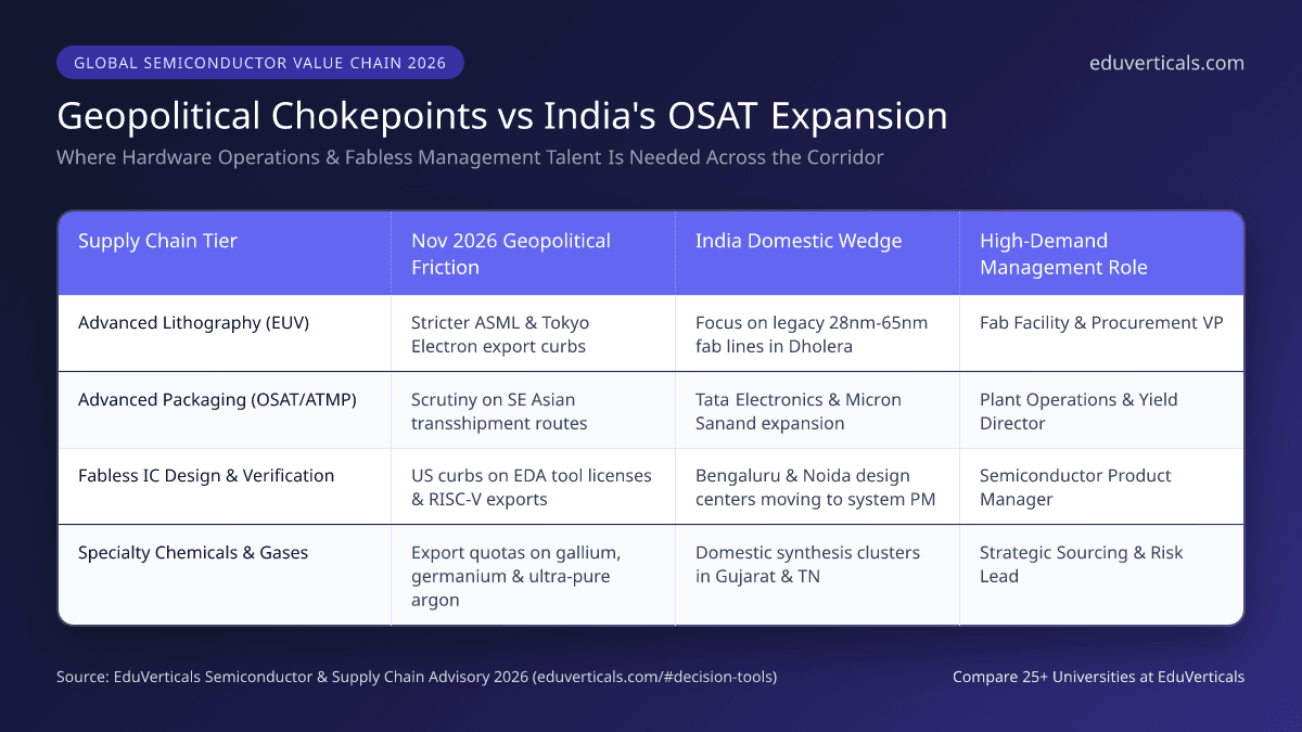
While front-end semiconductor fabrication (foundry production below 14nm) requires $10–$20 billion in capital and five to seven years of water and power stabilization, back-end Assembly, Testing, Marking, and Packaging (ATMP) and Outsourced Semiconductor Assembly and Test (OSAT) facilities deliver immediate commercial return on investment within 18 to 24 months. India’s strategic roadmap has recognized this fundamental reality:
Select your career goal to tailor advice
Focus on operations research, Six Sigma yield management, and cleanroom ERP systems to target Director of Fab Operations roles. Explore executive programmes on EduVerticals.
For decades, Indian microelectronics talent was concentrated in design centers across Bengaluru, Hyderabad, and Noida—performing digital layout and RTL verification for foreign multinationals. While India boasts over 20% of global chip designers, it has lacked leaders who understand plant operations, fab supply chains, and capital allocation.
When an OSAT facility experiences a packaging yield drop or shipping delay on ultra-pure molding compound, the problem is rarely an individual technical bug. It is an operations management crisis involving inventory carrying costs, liquidated damages, vendor penalty enforcement, and production rescheduling.
Hardware engineers who understand cleanroom physics but cannot read a corporate P&L balance sheet or model working capital requirements are finding themselves stalled at Senior Staff Engineer titles. In contrast, professionals who supplement their engineering degrees with an accredited postgraduate management qualification are moving straight into Plant General Manager, Director of Global Sourcing, and VP of Operations roles commanding packages exceeding ₹45L–₹75L.
Mid-career engineers working inside semiconductor design centers or manufacturing corridors cannot afford to resign for two full years of residential schooling—especially when hardware salaries and equity grants are escalating rapidly. That structural reality makes UGC-DEB entitled Online MBAs and Executive MBAs the premier upskilling route for engineering professionals.
By choosing NAAC A+ or A++ accredited institutions such as Manipal University Jaipur (MUJ) or NMIMS CDOE, working engineers master critical management frameworks while remaining fully employed on active projects. Core curriculum modules in Operations Management, Supply Chain Analytics, Strategic Procurement, and Corporate Finance directly inform daily cleanroom and vendor decisions.
Furthermore, for professionals aspiring to transition into regional leadership roles across Singapore, Tokyo, or Munich, these programmes offer verified WES equivalence, ensuring the credential holds global academic parity. You can evaluate curriculum tracks, fees, and semester EMI options directly on the EduVerticals Academic Catalog or test your projected 5-year salary trajectory using the .
Editorial BriefReading BriefTake the Next Step in Semiconductor Leadership: Explore specialized management programmes designed for engineering leaders on EduVerticals Course Catalog and speak with an enterprise career advisor today.
Keep the details close
Explore key programme specifications, recognition terms, fee components, and career outcomes side by side before applying.
Roles such as Director of Fab Operations, Head of Strategic Sourcing & Packaging Procurement, Semiconductor Product Line Manager, and Global Trade Compliance Lead command compensation packages ranging from ₹40 Lakhs to ₹90 Lakhs per annum plus performance incentives.
Bring programme options, estimated fees and study flexibility into one view, with the trade-offs and questions to verify.
Tailored shortlist from our admission partners. Verify fees and eligibility before applying.


We have a team of over 12 experienced mentors with over 26+ years of collective experience available to guide you at a moment's notice.